Industry’s first 100+ layer single-tier design for superior speed and power efficiency
[Mediapen=Cho Han-jin] Even among Japan’s economic retaliation, Samsung Electronics is strengthening its semiconductor technology, widening the gap with competitors.
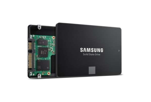
Samsung announced today that it has begun mass producing 250GB SATA SSD that integrates the company’s sixth-generation(1xx-layer) 256-GB three-bit V-NAND for global PC OEMs.
| |
 |
|
| ▲ Samsung-V6-SSD /Source=Samsung Electronics |
“By bringing cutting-edge 3D memory technology to volume production, we are able to introduce timely memory lineups that significantly raise the bar for speed and power efficiency,” said Kye Hyun Kyung, executive vice president of Solution Product & Development at Samsung Electronics.
With the industry’s fastest data transfer rate, Samsung’s sixth-generation V-NAND takes 3D memory to the next level.
Utilizing Samsung’s unique ‘channel hole etching’ technology, the new V-NAND adds around 40 percent more cells to the previous 9x-layer single-stack structure. This is achieved by building an electrically conductive mold stack comprised of 136 layers, then vertically piercing cylindrical holes from top to bottom, creating uniform 3D charge trap flash(CTF) cells.
As the mold stack in each cell area increases in height, NAND flash chips tend to become more vulnerable to errors and read latencies. To overcome such limitations, Samsung has incorporated a speed-optimized circuit design that allows it to achieve the fastest data transfer speed, at below 450 microseconds (μs) for write operations and below 45μs for reads. Compared to the previous generation, this represents a more than 10-percent improvement in performance, while power consumption is reduced by more than 15 percent.
Thanks to this speed-optimized design, Samsung will be able to offer next-generation V-NAND solutions with over 300 layers simply by mounting three of the current stacks without compromising chip performance or reliability.
In addition, the number of channel holes required to create a 256Gb chip density has decreased to 670 million holes from over 930 million with the previous generation, enabling reduced chip sizes and less process steps. This results in a more than 20-percent improvement in manufacturing productivity.
Leveraging the high-speed and low-power features, Samsung plans to broaden the reach of its 3D V-NAND into the automotive market where high reliability is extremely critical.